Introduction
- An interference microscope is an advanced optical instrument that utilizes the principles of light interference to enhance image contrast and measure minute variations in surface topology, thickness, and refractive index.
- It is particularly useful for examining unstained, transparent specimens in biological and material sciences.

- Unlike conventional light microscopes, which rely on absorption or scattering of light, interference microscopes detect phase differences in light waves passing through a specimen, providing high-resolution quantitative imaging.
- Developed from principles of phase contrast and interferometry, this microscope is widely used in scientific and industrial applications where precision is required, such as semiconductor inspection, biomedical imaging, and nanotechnology.
Working Principle
The interference microscope operates based on the principles of optical interference. It functions by splitting a light beam into two separate paths:
-
Object Beam – Passes through the specimen, acquiring phase information based on the optical properties of the sample.
-
Reference Beam – Does not pass through the specimen and is used as a baseline for comparison.
- After traversing their respective paths, these two beams are recombined at the detector, forming an interference pattern.
- This pattern arises due to phase differences between the beams, which occur due to variations in optical path length (thickness or refractive index of the sample).
- The resulting fringes provide precise quantitative data about the sample’s structure.
Types of Interference Microscopes
-
Michelson Interference Microscope – Uses a Michelson interferometer for beam splitting.
-
Mach-Zehnder Interference Microscope – Allows separate paths for object and reference beams, useful for studying dynamic processes.
-
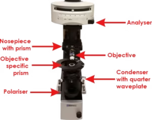
Nomarski (Differential Interference Contrast, DIC) Microscope – Uses prisms to generate and recombine polarized beams for enhanced edge contrast.
-
Phase-Shifting Interference Microscope – Incorporates a phase-shifting element to capture multiple interference patterns and reconstruct high-precision images.
Parts 
-
Illumination System
-
Light Source – Typically a laser, LED, or monochromatic light source for coherent illumination.
-
Condenser Lens – Focuses the light onto the sample.
-
-
Beam Splitting System
-
Beam Splitter – Divides the light into object and reference beams.
-
Reference Mirror – Reflects the reference beam back into the optical system.
-
-
Imaging System
-
Objective Lenses – Focus the object beam onto the detector.
-
Compensator/Phase Plate – Controls phase shifts for better contrast.
-
Interference Filter – Selects specific wavelengths to enhance contrast.
-
-
Detection and Analysis System
-
Eyepiece or Camera – Captures and displays the interference pattern.
-
Image Processing Software – Converts interference fringes into quantitative measurements.
-
Maintenance
To ensure optimal performance and longevity, regular maintenance is essential:
1. Optical Component Maintenance
-
Clean lenses and mirrors using lens paper and alcohol-based solutions to remove dust and oil.
-
Check beam splitter and prisms for any misalignment or contamination.
2. Mechanical Maintenance
-
Align the optical system regularly to maintain proper interference conditions.
-
Inspect stage movements for smooth operation and prevent mechanical wear.
3. Environmental Considerations
-
Keep in a vibration-free environment, as mechanical disturbances can affect interference patterns.
-
Control humidity and temperature, as optical properties may change due to environmental variations.
4. Software and Electronics Maintenance
-
Regularly update software for image processing.
-
Check and calibrate detectors and cameras for accurate image capture.
Applications
1. Biomedical and Biological Applications
-
Imaging live cells without the need for staining.
-
Measuring cell membrane thickness and intracellular structures.
-
Analyzing biomolecular interactions in real-time.
2. Material Science and Nanotechnology
-
Measuring thin film thickness in semiconductor industries.
-
Inspecting surface roughness and defects in metals and coatings.
-
Studying crystal growth and microstructures.
3. Optical and Semiconductor Industry
-
Inspecting integrated circuits and MEMS devices.
-
Measuring lens and mirror surface imperfections.
4. Metrology and Surface Profiling
-
High-precision surface height measurements in engineering.
-
Analyzing wear and tear in mechanical components.
5. Forensic and Chemical Analysis
-
Examining microscopic evidence in forensic science.
-
Studying chemical reaction kinetics using interference patterns.
Advantages
- High Resolution & Precision – Measures nanometer-scale variations in surface topography and refractive index.
- Non-Destructive Analysis – Suitable for live-cell imaging and delicate samples.
- Enhanced Contrast – Provides detailed images of unstained, transparent specimens.
- Quantitative Measurements – Enables thickness and refractive index calculations.
- Wide Range of Applications – Useful in biology, materials science, and industrial quality control.
Disadvantages and Limitations
- Complex Setup – Requires precise alignment and calibration.
- Expensive – High costs compared to conventional light microscopes.
- Vibration Sensitivity – Susceptible to external mechanical disturbances.
- Limited Sample Types – Works best for thin, transparent samples; opaque materials require modifications.
- Difficult Interpretation – Interference patterns require expertise for accurate analysis.